Bias Current Source ≲25nA
3 US Patents Issued & Proof of Silicon
Bias Current Sources with Positive Temperature Coefficient: This section contains a number of ultra-low-power (e.g., nano-ampere) “Proportional to Absolute Temperature” (PTAT) current sources (IPTAT), which have a positive temperature coefficient (TC) and can be fabricated in standard digital CMOS. IPTAT current sources are fundamental building blocks, generally providing a lifeline for other analog circuits (e.g., amplifiers, voltage references, ADCs, DACs, etc.). As such, Ai Linear offers numerous proprietary IPTAT intellectual property (IP) cells tailored to the different needs of other analog circuits they serve. These needs include less dependence on PMOSFETs vs. NMOSFETs, low operating VDD vs. low voltage coefficient, PTAT loops coupled to VDD or VSS, etc. The IPTAT circuits also include a start-up and power-off feature. Some of the common traits of IPTAT circuits are summarized below. Please contact sales@ailinear.com for more information.
The intellectual property (IP) cells are generally portable from trailing-edge to bleeding-edge CMOS.
- Tiny CMOS bias current cell with positive temperature coefficient (TC) operating in subthreshold with ultra-low current consumption (IDD).
- Large value but tiny active bias resistor (RA) keeps IDD ultra-low.
- IDD and IOUT absolute values are mostly a function of MOSFET mobility (µ), inherently more stable to help narrow IDD variation over fabrication process corners.
- Diverting most leakages (of RA and key FETs) to supplies to improve the temperature range.
- No clock, no switch-capacitor, and no related noise or injections into the substrate.
- Narrow variations over manufacturing processes are also due to IDD and IOUT being less sensitive to VTH.
- No passive resistors and no passive capacitors keep the area small and silicon cost low.
- IOUT can be calibrated or trimmed for TC.
- Programmable (pre- or post-silicon) IOUT that tracks IDD.

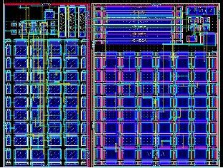
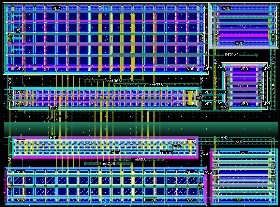
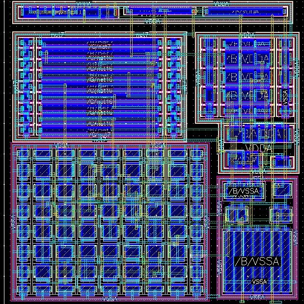
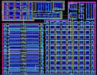
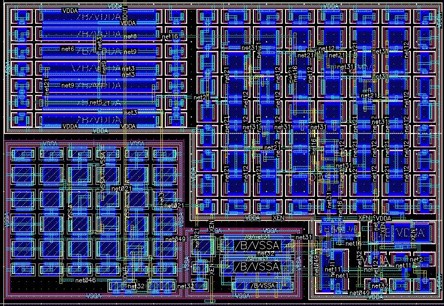
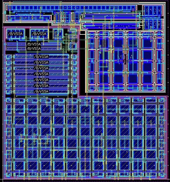


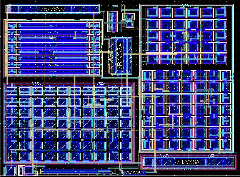

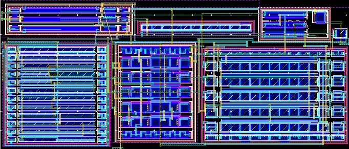

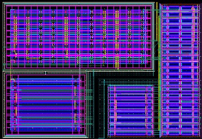
Bias Current Cell Table Summary
Proof of Silicon Preliminary Specifications
Refer to each cell data sheet below for more details (please see disclaimers)
| Cell Name | TSMC Fab Node | Cell Size (µm × µm) | VDD High (V) | VDD Low (V) | IDD (nA) | +TC (%/C) | +VC (%/V) | Comments |
|---|---|---|---|---|---|---|---|---|
| IBIAS3A | 180nm | 94 × 41 | 2 | 0.8 | 9 | 0.5 | 0.5 | Utilizes RPMOS, PTAT KCL coupled to VDD |
| IBIAS3B | 180nm | 64 × 57 | 2 | 0.8 | 7 | 0.3 | 0.4 | Utilizes RPMOS, PTAT KCL coupled to VDD |
| IBIAS3C | 180nm | 110 × 80 | 2 | 0.8 | 7 | 0.6 | 0.3 | Utilizes RPMOS, PTAT KCL coupled to VDD, Multiple IOUT ports |
| IBIAS4 | 180nm | 48 × 50 | 2 | 0.7 | 6 | 0.5 | 0.5 | Utilizes RPMOS, PTAT KCL coupled to VSS |
| IBIAS5 | 180nm | 62 × 48 | 2 | 0.8 | 11 | 0.4 | 0.5 | Utilizes RNMOS, PTAT KCL coupled to VSS |
| IBIAS8 | 180nm | 60 × 40 | 2 | 0.9 | 7 | 0.5 | 0.3 | Utilizes RPMOS, PTAT KCL coupled to VDD |
| IBIAS9 | 180nm | 60 × 65 | 2 | 0.8 | 15 | 0.4 | 0.3 | Utilizes RNMOS, PTAT KCL coupled to VSS |
| IBIAS9A | 180nm | 64 × 60 | 2 | 0.8 | 7 | 0.5 | 0.3 | Utilizes RNMOS, PTAT KCL coupled to VSS |
| IBIAS10 | 180nm | 80 × 40 | 2 | 0.8 | 19 | 0.3 | 0.4 | Utilizes RNMOS, PTAT KCL coupled to VDD |
| IBIAS11 | 180nm | 68 × 50 | 2 | 0.8 | 12 | 0.4 | 0.4 | Utilizes RPMOS, PTAT KCL coupled to VSS |
| IBIAS11A | 180nm | 68 × 52 | 2 | 0.7 | 12 | 0.4 | 0.4 | Utilizes RPMOS, PTAT KCL coupled to VSS |
| IBIAS12L | 180nm | 90 × 40 | 2 | 0.8 | 22 | 0.7 | 0.4 | Utilizes RPMOS, PTAT KCL coupled to VDD |
| IBIAS13 | 65nm | 60 × 30 | 1 | 0.6 | 10 | 0.6 | 0.5 | Utilizes RNMOS, PTAT KCL coupled to VSS |
| IBIAS14 | 65nm | 45 × 30 | 1 | 0.6 | 13 | 0.6 | 0.5 | Utilizes RPMOS, PTAT KCL coupled to VDD |
IBIAS3A Features (proof of silicon available):
- View Data-Sheet
- Programmable (pre- or post-silicon) IOUT that tracks IDD.
- Tiny CMOS (~91μm × 41μm) bias current Intellectual Property (IP) cell operating in subthreshold with ultra-low current consumption IDD (typical 9nA).
- Large value but tiny active bias resistor (RPMOS) as a function of PMOSFET keeps IDD ultra-low.
- Most suitable for SoC (System on Chip) applications where analog (e.g., oscillator, comparator, ADC) performance best correlates with PMOSFET parameters.
- Utilizing cascode current mirrors (1VGS + 2VDS) for lower operating VDD.
- Suitable for SoC where IBIAS is more optimized when the PTAT Kirchhoff Voltage Loop (KVL) is coupled to VDD.
- IDD and IOUT absolute values are mostly a function of PMOSFET mobility (µ), inherently more stable, helping to narrow IDD variation over fabrication process corners.
- Based on 180nm digital CMOS at TSMC, portable to smaller fabrication nodes.
IBIAS3B Features (proof of silicon available):
- View Data-Sheet
- Programmable (pre- or post-silicon) IOUT that tracks IDD.
- Tiny CMOS (~64μm × 57μm) bias current Intellectual Property (IP) cell operating in subthreshold with ultra-low current consumption IDD (typical 7nA).
- Large value but tiny active bias resistor (RPMOS) as a function of PMOSFET keeps IDD ultra-low.
- Most suitable for SoC (System on Chip) applications where analog (e.g., oscillator, comparator, ADC) performance best correlates with PMOSFET parameters.
- Utilizing Wilson Current Mirrors (2VDD + 2VDS) for better voltage VDD coefficient.
- Suitable for SoC where IBIAS is more optimized when the PTAT Kirchhoff Voltage Loop (KVL) is coupled to VDD.
- IDD and IOUT absolute values are mostly a function of PMOSFET mobility (µ), inherently more stable, helping to narrow IDD variation over fabrication process corners.
- Based on 180nm digital CMOS at TSMC, portable to smaller fabrication nodes.
IBIAS3C Features (proof of silicon available):
- View Data-Sheet
- 6 positive (from VDD) and negative (from VSS) output IOUT ports.
- Programmable (pre- or post-silicon) IOUT that tracks IDD.
- Tiny CMOS (~110μm × 80μm) bias current Intellectual Property (IP) cell operating in subthreshold with ultra-low current consumption IDD (typical 30nA).
- Large value but tiny active bias resistor (RPMOS) as a function of PMOSFET keeps IDD ultra-low.
- Most suitable for SoC (System on Chip) applications where analog (e.g., oscillator, comparator, ADC) performance best correlates with PMOSFET parameters.
- Utilizing Wilson Current Mirrors (2VDD + 2VDS) for better voltage VDD coefficient.
- Suitable for SoC where IBIAS is more optimized when the PTAT Kirchhoff Voltage Loop (KVL) is coupled to VDD.
- IDD and IOUT absolute values are mostly a function of PMOSFET mobility (µ), inherently more stable, helping to narrow IDD variation over fabrication process corners.
- Based on 180nm digital CMOS at TSMC, portable to smaller fabrication nodes.
IBIAS4 Features (proof of silicon available):
- View Data-Sheet
- Patented.
- Programmable (pre- or post-silicon) IOUT that tracks IDD.
- Tiny CMOS (~48μm × 50μm) bias current Intellectual Property (IP) cell operating in subthreshold with ultra-low current consumption IDD (typical 6nA).
- Large value but tiny active bias resistor (RPMOS) as a function of PMOSFET keeps IDD ultra-low.
- Most suitable for SoC (System on Chip) applications where analog (e.g., oscillator, comparator, ADC) performance best correlates with PMOSFET parameters.
- Suitable for SoC where IBIAS is more optimized when VSS is coupled with PTAT Kirchhoff Voltage Loop (KVL).
- Utilizing PTAT loop with NMOSFETs needing 1VGS + 2VDS for lower VDD operating range.
- IDD and IOUT absolute values are mostly a function of PMOSFET mobility (µ), inherently more stable, helping to narrow IDD variation over fabrication process corners.
IBIAS5 Features (proof of silicon available):
- View Data-Sheet
- Patented.
- Programmable (pre- or post-silicon) IOUT that tracks IDD.
- Tiny CMOS (~62μm × 48μm) bias current Intellectual Property (IP) cell operating in subthreshold with ultra-low current consumption IDD (typical 11nA).
- Large value but tiny active bias resistor (RNMOS) as a function of NMOSFET keeps IDD ultra-low.
- Most suitable for SoC (System on Chip) applications where analog (e.g., oscillator, comparator, ADC) performance best correlates with NMOSFET parameters.
- Suitable for SoC where IBIAS is more optimized when VSS is coupled with PTAT Kirchhoff Voltage Loop (KVL).
- Utilizing PTAT loop with NMOSFETs needing 1VGS + 2VDS for lower VDD operating range.
- IDD and IOUT absolute values are mostly a function of NMOSFET mobility (µ), inherently more stable, helping to narrow IDD variation over fabrication process corners.
IBIAS8 Features (proof of silicon available):
- View Data-Sheet
- Programmable (pre- or post-silicon) IOUT that tracks IDD.
- Tiny CMOS (~60μm × 40μm) bias current Intellectual Property (IP) cell operating in subthreshold with ultra-low current consumption IDD (typical 11nA).
- Large value but tiny active bias resistor (RPMOS) as a function of PMOSFET keeps IDD ultra-low.
- Most suitable for SoC (System on Chip) applications where analog (e.g., oscillator, comparator, ADC) performance best correlates with PMOSFET parameters.
- Utilized regulated cascode current mirrors (RGC) to enhance IBIAS voltage VDD coefficient.
- Suitable for SoC where IBIAS is more optimized when PTAT Kirchhoff Voltage Loop (KVL) is coupled to VDD.
- IDD and IOUT absolute values are mostly a function of PMOSFET mobility (µ), inherently more stable, helping to narrow IDD variation over fabrication process corners.
IBIAS9 Features (proof of silicon available):
- View Data-Sheet
- Programmable (pre- or post-silicon) IOUT that tracks IDD.
- Tiny CMOS (~60μm × 65μm) bias current Intellectual Property (IP) cell operating in subthreshold with ultra-low current consumption IDD (typical 15nA).
- Large value but tiny active bias resistor (RPMOS) as a function of NMOSFET keeps IDD ultra-low.
- Most suitable for SoC (System on Chip) applications where analog (e.g., oscillator, comparator, ADC) performance best correlates with NMOSFET parameters.
- Utilizing cascode current mirrors (1VGS + 2VDS) for lower operating VDD.
- Suitable for SoC where IBIAS is more optimized when PTAT Kirchhoff Voltage Loop (KVL) is coupled to VSS.
- IDD and IOUT absolute values are mostly a function of NMOSFET mobility (µ), inherently more stable, helping to narrow IDD variation over fabrication process corners.
- Based on 180nm digital CMOS at TSMC, portable to smaller fabrication nodes.
IBIAS9A Features (proof of silicon available):
- View Data-Sheet
- Programmable (pre- or post-silicon) IOUT that tracks IDD.
- Tiny CMOS (~60μm × 64μm) bias current Intellectual Property (IP) cell operating in subthreshold with ultra-low current consumption IDD (typical 7nA).
- Large value but tiny active bias resistor (RPMOS) as a function of NMOSFET keeps IDD ultra-low.
- Most suitable for SoC (System on Chip) applications where analog (e.g., oscillator, comparator, ADC) performance best correlates with NMOSFET parameters.
- Utilizing Wilson PMOS current mirrors (2VGS + 2VDS) for improved voltage VDD coefficient.
- Suitable for SoC where IBIAS is more optimized when PTAT Kirchhoff Voltage Loop (KVL) is coupled to VSS.
- IDD and IOUT absolute values are mostly a function of NMOSFET mobility (µ), inherently more stable, helping to narrow IDD variation over fabrication process corners.
- Based on 180nm digital CMOS at TSMC, portable to smaller fabrication nodes.
IBIAS10 Features (proof of silicon available):
- View Data-Sheet
- Patented
- Programmable (pre- or post-silicon) IOUT that tracks IDD.
- Tiny CMOS (~80μm × 40μm) bias current Intellectual Property (IP) cell operating in subthreshold with ultra-low current consumption IDD (typical 19nA).
- Large value but tiny active bias resistor (RNMOS) as a function of NMOSFET keeps IDD ultra-low.
- Most suitable for SoC (System on Chip) applications where analog (e.g., oscillator, comparator, ADC) performance best correlates with NMOSFET parameters.
- Suitable for SoC where IBIAS is more optimized when VDD is coupled with PTAT Kirchhoff Voltage Loop (KVL).
- Utilizing PTAT loop with PMOSFETs needing 1VGS + 2VDS for lower VDD operating range.
- IDD and IOUT absolute values are mostly a function of NMOSFET mobility (µ), inherently more stable, helping to narrow IDD variation over fabrication process corners.
- Based on 180nm digital CMOS at TSMC, portable to smaller fabrication nodes.
IBIAS11 Features (proof of silicon available):
- View Data-Sheet
- Patented
- Programmable (pre- or post-silicon) IOUT that tracks IDD.
- Tiny CMOS (~68μm × 50μm) bias current Intellectual Property (IP) cell operating in subthreshold with ultra-low current consumption IDD (typical 12nA).
- Large value but tiny active bias resistor (RPMOS) as a function of PMOSFET keeps IDD ultra-low.
- Most suitable for SoC (System on Chip) applications where analog (e.g., oscillator, comparator, ADC) performance best correlates with PMOSFET parameters.
- Suitable for SoC where IBIAS is more optimized when VSS is coupled with PTAT Kirchhoff Voltage Loop (KVL).
- Utilizing PTAT loop with NMOSFETs needing 1VGS + 2VDS for lower VDD operating range.
- IDD and IOUT absolute values are mostly a function of PMOSFET mobility (µ), inherently more stable, helping to narrow IDD variation over fabrication process corners.
- Based on 180nm digital CMOS at TSMC, portable to smaller fabrication nodes.
IBIAS11A Features (proof of silicon available):
- View Data-Sheet
- Patented
- Programmable (pre- or post-silicon) IOUT that tracks IDD.
- Tiny CMOS (~68μm × 52μm) bias current Intellectual Property (IP) cell operating in subthreshold with ultra-low current consumption IDD (typical 12nA).
- Large value but tiny active bias resistor (RPMOS) as a function of PMOSFET keeps IDD ultra-low.
- Most suitable for SoC (System on Chip) applications where analog (e.g., oscillator, comparator, ADC) performance best correlates with PMOSFET parameters.
- Suitable for SoC where IBIAS is more optimized when VSS is coupled with PTAT Kirchhoff Voltage Loop (KVL).
- Utilizing PTAT loop with NMOSFETs needing 1VGS + 2VDS for lower VDD operating range.
- IDD and IOUT absolute values are mostly a function of PMOSFET mobility (µ), inherently more stable, helping to narrow IDD variation over fabrication process corners.
IBIAS12L Features (proof of silicon available):
- View Data-Sheet
- Programmable (pre or post silicon) IOUT that tracks IDD
- Tiny CMOS (~90μm×40 μm) bias current Intellectual Property (IP) cell operating in subthreshold with ultra-low current consumption IDD (typical 22nA)
- Large value but tiny active bias resistor (RPMOS) as a function of PMOSFET keeps IDDultra-low
- Most suitable for SoC whose analog (e.g., oscillator, comparator, ADC) performance best correlates with PMOSFET parameters
- Utilizing peaking current mirrors (1VGS+2VDS) for lower voltage VDD coefficient and lower operating VDD
- Suitable for SoC where IBIAS is more optimized when PTAT Kirkoff Voltage Loop (KVL) is coupled to VDD
- IDD and IOUT absolute value mostly a function of PMOSFET mobility (µ) inherently more stable to help narrow IDD variation over fabrication process corners
- Based on 180nm digital CMOS at TSMC and portable to smaller fabrication nodes.
IBIAS13 Features (proof of silicon available):
- View Data-Sheet
- Programmable (pre- or post-silicon) IOUT that tracks IDD.
- Tiny CMOS (~60μm × 30μm) bias current Intellectual Property (IP) cell operating in subthreshold with ultra-low current consumption IDD (typical 10nA).
- Large value but tiny active bias resistor (RPMOS) as a function of NMOSFET keeps IDD ultra-low.
- Most suitable for SoC (System on Chip) applications where analog (e.g., oscillator, comparator, ADC) performance best correlates with NMOSFET parameters.
- Utilizing cascode current mirrors (1VGS + 2VDS) for lower operating VDD.
- Suitable for SoC where IBIAS is more optimized when PTAT Kirchhoff Voltage Loop (KVL) is coupled to VSS.
- IDD and IOUT absolute values are mostly a function of NMOSFET mobility (µ), inherently more stable, helping to narrow IDD variation over fabrication process corners.
- Based on 65nm digital CMOS at TSMC and portable to smaller fabrication nodes.
IBIAS14 Features (proof of silicon available):
- View Data-Sheet
- Programmable (pre- or post-silicon) IOUT that tracks IDD.
- Tiny CMOS (~45μm × 30μm) bias current Intellectual Property (IP) cell operating in subthreshold with ultra-low current consumption IDD (typical 13nA).
- Large value but tiny active bias resistor (RPMOS) as a function of PMOSFET keeps IDD ultra-low.
- Most suitable for SoC (System on Chip) applications where analog (e.g., oscillator, comparator, ADC) performance best correlates with PMOSFET parameters.
- Utilizing cascode current mirrors (1VGS + 2VDS) for lower operating VDD.
- Suitable for SoC where IBIAS is more optimized when PTAT Kirchhoff Voltage Loop (KVL) is coupled to VDD.
- IDD and IOUT absolute values are mostly a function of PMOSFET mobility (µ), inherently more stable, helping to narrow IDD variation over fabrication process corners.
- Based on 65nm digital CMOS at TSMC and portable to smaller fabrication nodes.
