
Voltage References ≲350nA
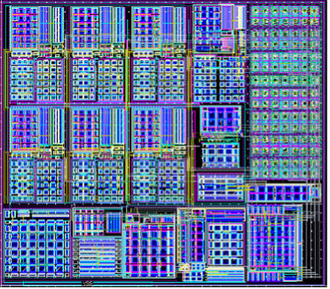
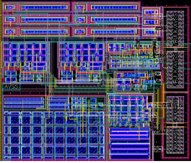
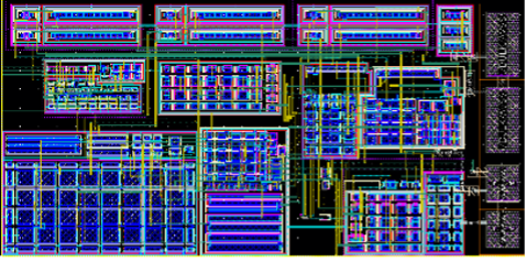
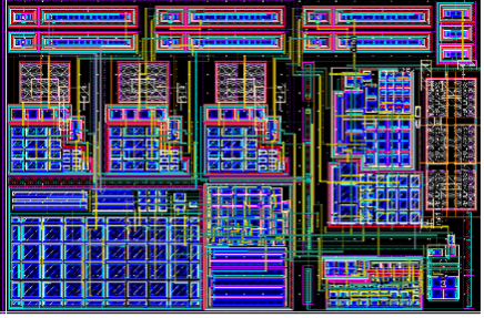
2 US Patents Issued & Proof of Silicon
Voltage References (VREF) & VREF + IREF in one with Low Temperature Coefficient (TC): This section contains a number of CMOS ultra-low power (e.g. nano-ampere) VREFs and VREF + IREF combined, having low TCs. The VREFs offered here are bandgap (e.g., VREF≈VBG≈1.2), fractional bandgap (e.g., VREF≈VBG/2≈0.6), and fractional (VREF≈0.4v) and the TC can be programmed or trimmed. The VREF and IREF circuits include start-up and a power-off capability as well. VREFs generally includes an internal buffer (BUF) to drive larger loads (e.g. Mega Ωs) in a SoC. Some of the common traits of VREF & IREF circuits are summarized below. Testing is ongoing, with specific performance metrics labeled as TBD. Please contact sales@ailinear.com for more information or to order specific testing.
- Bandgap voltage (including fractional VBG) and current reference cells, in standard digital CMOS, having low TC while operating in subthreshold at ultra-low current consumption IDD
- No clock, no switch-capacitor, and no related noise or injections into substrate
- Narrow variations over process also due to VREF and IREFless sensitivity to VTH
- The Intellectual Property (IP) cells here are generally portable from trailing-to-bleeding edge CMOS


Voltage Reference Cell Table Summary
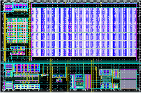
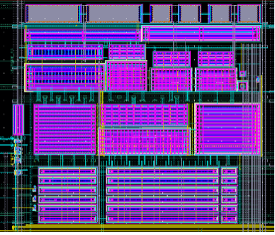
Proof of Silicon Preliminary Specifications
Refer to each cell data sheet below for more details (please see disclaimers)
| Cell Name | TSMC Fab Node | Cell Size (µm × µm) | VDD High (V) | VDD Low (V) | IDD (nA) | VREF (V) | TC (PPM/C) | VC (dB) | Comments |
|---|---|---|---|---|---|---|---|---|---|
| VREF1 | 180nm | 180 × 150 | 2 | 1.5 | 153 | 1.28 | 150 | 68 | No resistors & low noise |
| VREF2 | 180nm | 100 × 85 | 2 | 0.7 | 25 | 0.43 | 350 | 76 | No resistors |
| VREF3 | 180nm | 144 × 77 | 2 | 0.7 | 26 | 0.44 | 340 | 74 | No resistors |
| VREF4 | 180nm | 132 × 87 | 2 | 0.7 | 29 | 0.43 | 230 | 69 | No resistors |
| VREF5 | 180nm | 460 × 250 | 2 | 1 | 270 | 0.63 | TBD | TBD | Fractional Bandgap VREF, Test in progress |
| VREF6 | 180nm | 440 × 290 | 1 | 1 | 290 | 0.63 | TBD | TBD | Fractional Bandgap VREF, Test in progress |
| VREF7+IREF | 65nm | 200 × 130 | 1 | 0.8 | 330 | 0.63 | TBD | TBD | Fractional Bandgap VREF & IREF (50nA typ), Test in progress |
| VREF8 | 65nm | 100 × 82 | 1 | 0.7 | 49 | 0.43 | TBD | TBD | No resistors, Test in progress |
VREF1 Features (proof of silicon available):
- View Datasheet
- Small CMOS (~180μm×150 μm) bandgap voltage reference (VOUT ≈ VREF ≈ VBG ≈ 1.28) Intellectual Property (IP) cell operates in subthreshold with ultra-low IDD (typical 153nA)
- Patented Low noise design to generate proportional to absolute voltage (VPTAT) without resistors
- Equipped with start-up, power-down, and TC trim capability
- Includes an internal buffer (BUF) to drive larger loads (e.g. Mega Ωs) in a SoC
- No clock, no switch-capacitor, and no related noise or injections into substrate
- Operating in subthreshold and requiring no resistors facilitate small silicon area and operations at ultra-low currents
- Operation at low VDD levels ≈VREF + 2VDS
- Utilizes parasitic (substrate) bipolar junction transistor (BJT) freely available in digital CMOS
- Manufacturable on trailing-to-bleeding edge digital CMOS
- Based on 180nm digital CMOS at TSMC and portable to smaller fabrication nodes.
- patented
VREF2 Features (proof of silicon available):
- View Datasheet
- Small CMOS (~100μm×85 μm) bandgap voltage reference (VOUT ≈ VREF ≈ 0.43) Intellectual Property (IP) cell operates in subthreshold with ultra-low IDD (typical 25nA)
- Patented Low noise design to generate proportional to absolute voltage (VPTAT) without resistors
- Equipped with start-up, power-down, and TC trim capability
- Includes an internal buffer (BUF) to drive larger loads (e.g. Mega Ωs) in a SoC
- No clock, no switch-capacitor, and no related noise or injections into substrate
- Operating in subthreshold and requiring no resistors facilitate small silicon area and operations at ultra-low currents
- Operation at low VDD levels ≈VREF + 2VDS
- Manufacturable on trailing-to-bleeding edge digital CMOS
- Based on 180nm digital CMOS at TSMC and portable to smaller fabrication nodes.
- Patented
VREF3 Features (proof of silicon available):
- View Datasheet
- Small CMOS (~144μm×77 μm) bandgap voltage reference (VOUT ≈ VREF ≈ 0.44) Intellectual Property (IP) cell operates in subthreshold with ultra-low IDD (typical 26nA)
- Patented Low noise design to generate proportional to absolute voltage (VPTAT) without resistors
- Equipped with start-up, power-down, and TC trim capability
- Includes an internal buffer (BUF) to drive larger loads (e.g. Mega Ωs) in a SoC
- No clock, no switch-capacitor, and no related noise or injections into substrate
- Operating in subthreshold and requiring no resistors facilitate small silicon area and operations at ultra-low currents
- Operation at low VDD levels ≈VREF + 2VDS
- Manufacturable on trailing-to-bleeding edge digital CMOS
- Based on 180nm digital CMOS at TSMC and portable to smaller fabrication nodes.
- Patented
VREF4 Features (proof of silicon available):
- View Datasheet
- Small CMOS (~132μm×87 μm) bandgap voltage reference (VOUT ≈ VREF ≈ 0.43v) Intellectual Property (IP) cell operates in subthreshold with ultra-low IDD (typical 29nA)
- Patented Low noise design to generate proportional to absolute voltage (VPTAT) without resistors
- Equipped with start-up, power-down, and TC trim capability
- Includes an internal buffer (BUF) to drive larger loads (e.g. Mega Ωs) in a SoC
- No clock, no switch-capacitor, and no related noise or injections into substrate
- Operating in subthreshold and requiring no resistors facilitate small silicon area and operations at ultra-low currents
- Operation at low VDD levels ≈VREF + 2VDS
- Manufacturable on trailing-to-bleeding edge digital CMOS
- Based on 180nm digital CMOS at TSMC and portable to smaller fabrication nodes.
- Patented
VREF5 Features (proof of silicon available):
- View Datasheet
- CMOS (~460μm×250 μm) fractional bandgap voltage reference (VOUT ≈ VREF ≈ 0.5VBG ≈ 0.63) Intellectual Property (IP) cell operates in subthreshold with low IDD (typical 270nA)
- Trimmable or Programmable (pre or post silicon) absolute value of VREF
- Trimmable or Programmable TC
- Equipped with start-up, and power-down
- Includes an internal buffer (BUF) to drive larger loads (e.g. Mega Ωs) in a SoC
- No clock, no switch-capacitor, and no related noise or injections into substrate
- Utilizes a fractional bandgap topology to generate IREF through a bias resistor (RPOLY)
- Operation at low VDD levels ≈VREF + 2VDS
- Suitable for SoC optimized for IREF fractional bandgap voltage loop that is coupled to VSS
- Utilizes parasitic (substrate) bipolar junction transistor (BJT) freely available in digital CMOS
- Based on 180nm digital CMOS at TSMC and portable to smaller fabrication nodes.
- Patented
VREF6 Features (proof of silicon available):
- View Datasheet
- CMOS (~440μm×290 μm) fractional bandgap voltage reference (VOUT ≈ VREF ≈ 1/2VBG ≈ 0.63) Intellectual Property (IP) cell operates in subthreshold with low IDD (typical 290nA)
- Trimmable or Programmable (pre or post silicon) absolute value of VREF
- Trimmable or Programmable TC
- Equipped with start-up, and power-down
- Includes an internal buffer (BUF) to drive larger loads (e.g. Mega Ωs) in a SoC
- No clock, no switch-capacitor, and no related noise or injections into substrate
- Utilizes a fractional bandgap topology to generate IREF through a bias resistor (RPOLY)
- Operation at low VDD levels ≈VREF + 2VDS
- Suitable for SoC optimized for IREF fractional bandgap voltage loop that is coupled to VSS
- Utilizes parasitic (substrate) bipolar junction transistor (BJT) freely available in digital CMOS
- Based on 180nm digital CMOS at TSMC and portable to smaller fabrication nodes.
- Patented
VREF7 Features (proof of silicon available):
- View Datasheet
- CMOS (~200μm×130 μm) fractional bandgap voltage and current reference (VREF ≈ VOUT ≈ 0.5VBG ≈ 0.63 & typ. IREF ≈ IOUT ≈ 50nA) Intellectual Property (IP) cell operates in subthreshold with low IDD (typical 330nA)
- Trimmable or Programmable (pre or post silicon) absolute value of VREF & IREF
- Trimmable or Programmable TC
- Equipped with start-up, and power-down
- VREF Includes an internal buffer (BUF) to drive larger loads (e.g. Mega Ωs) in a SoC
- No clock, no switch-capacitor, and no related noise or injections into substrate
- Utilizes a fractional bandgap topology to generate VREF & IREF through a bias resistor (RPOLY)
- Operation at low VDD levels ≈VREF + 2VDS
- Suitable for SoC optimized for VREF & IREF fractional bandgap voltage loop that is coupled to VSS
- Utilizes parasitic (substrate) bipolar junction transistor (BJT) freely available in digital CMOS
- Based on 65nm digital CMOS at TSMC and portable to smaller fabrication nodes.
- Patented
VREF8 Features (proof of silicon available):
- View Datasheet
- Small CMOS (~100μm×82 μm) bandgap voltage reference (VOUT ≈ VREF ≈ 0.43) Intellectual Property (IP) cell operates in subthreshold with ultra-low IDD (typical 49nA)
- Patented Low noise design to generate proportional to absolute voltage (VPTAT) without resistors
- Equipped with start-up, power-down, and TC trim capability
- Includes an internal buffer (BUF) to drive larger loads (e.g. Mega Ωs) in a SoC
- No clock, no switch-capacitor, and no related noise or injections into substrate
- Operating in subthreshold and requiring no resistors facilitate small silicon area and operations at ultra-low currents
- Operation at low VDD levels ≈VREF + 2VDS
- Manufacturable on trailing-to-bleeding edge digital CMOS
- Based on 65nm digital CMOS at TSMC and portable to smaller fabrication nodes.
- Patented