Introducing the Smart Amplifier (sAMP) series: an innovative range of patented CMOS amplifiers optimized for ultra-low power consumption, low noise, and moderate-speed operation. Designed to run in an ultra-low-power (e.g., 100nA), low-noise mode during steady-state conditions, these amplifiers seamlessly switch to high-speed operation when sensors detect a change, making them ideal for ‘always-on’ smart IoT and near-sensor AI applications. These amplifiers are essential in diverse industries, from consumer electronics and medical devices to micro-robotics and drones.
The sAMP family specifically targets the ultra-low-power, low-cost market segment, catering to applications where continuous, efficient monitoring is critical. The sAMP family includes start-up and power-off mechanisms. It also has an internal buffer to drive larger loads (e.g., 10s of Mega Ωs) in a low-power system-on-chip (SoC) environment. Testing of specific performance metrics is ongoing, with results forthcoming. For more information or to request testing, please contact us at sales@ailinear.com. Summary of the sAMP family traits are as follows:
Low-noise buffer-amplifier with near rail-to-rail input-output and (class AB) push-pull output stage
Patented method enables lowering noise in steady-state by an order of magnitude under apples-to-apples IQ operating currents while boosting slew-rate and settling-time in the face of imbalanced inputs
Topology retains inherent FCTA traits: optimal PSRR and CMRR, and fast slew-rate and settling-time considering ultra-low operating currents
Requiring neither passive capacitors nor resistors, lowers silicon cost and facilitates operations in subthreshold at ultra-low current
The sAMP input stage can be calibrated or trimmed to improve input offset voltage. Typical VOFFSET ≈ ±5mv
Typical VDDHIGH ≈ 2v for 180nm & ≈1v for 65nm;
Typical VINPUT & VOUTPUT swing from power supply rails ≈ ±50mv for 180nm and ≈ ±25mv for 65nm
Equipped with start-up, and power-down
Includes an internal buffer (BUF) to drive larger loads (e.g. Mega Ωs) in a SoC
Operating in subthreshold and requiring no resistors facilitate small silicon area and operations at ultra-low currents
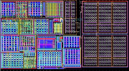
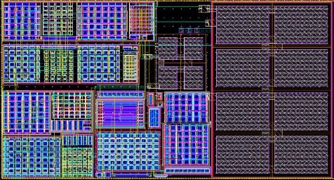
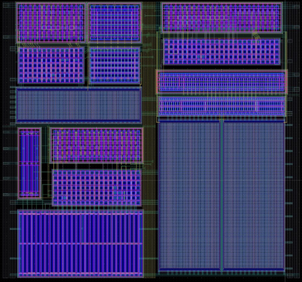
Based on 180nm & 65nm digital CMOS at TSMC and portable to smaller fabrication nodes.
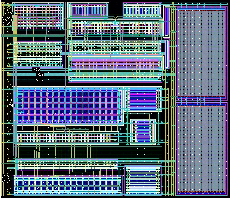
AMP1_1 - 100µm x 200µm
AMP1_2 - 105µm x 190µm
AMP1_3 - 100µm x 175µm
AMP3&4_1 - 160µm x 140µm
AMP3&4_2 - 165µm x 145µm
AMP2_0-105umX110um
AMP2_1 - 110µm x 100µm
AMP2_2-125umX100um
AMP2_3-115umX100]um
Smart Amplifier Family Table Summary
Proof of Silicon Preliminary Specifications
Refer to each cell data sheet below for more details (please see disclaimers)
Name
TSMC Fab Node
Cell Size (µm × µm)
IDD (nA)
Gain (dB)
PSRR (dB)
10Hz VO Noise (μV/√Hz)
fu (KHz)
SR (v/ms)
ts (μs)
AMP1_1
180nm
100 × 200
110
88
90
5
3
68
<50
AMP1_2
180nm
105 × 190
130
80
90
7
2
130
<25
AMP1_3
180nm
100 × 175
90
85
90
4
1
72
<50
AMP3&4_1
180nm
160 × 140
95
95
85
6
5
121
<35
AMP3&4_2
180nm
165 × 145
127
85
80
7
1
74
<60
AMP2_0
65nm
105 × 110
82
92
92
7
8
150
<30
AMP2_1
65nm
110 × 100
60
90
90
7
5
70
<60
AMP2_2
65nm
125 × 100
100
88
80
8
7
140
<30
AMP2_3
65nm
115 × 100
73
90
80
7
7
170
<20
Notes: All sAMPs Fabricated in low-cost Digital CMOS. All sAMPs VOFFSET in the ~±5mV range without trim. Testing temperature ~ 27°C. External RLOAD utilized to increase quiescent current of sAMP buffer output in order to drive measurement gear load. Test condition for high VDD~2V for 180nm & VDD~1V for 65nm. Test conditions for low VDD~1.2V for 180nm & VDD~0.8V for 65nm. Temp test in progress. Gain and PSRR measured at higher frequencies and extrapolated back for gain at DC.
AMP1_1: Features (proof of 180nm silicon available):