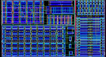
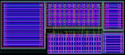
Current References ≲150nA
5 US Patents Issues & Proof of Silicon
Current References (IREF) with Low Temperature Coefficient (TC): This section contains a number of CMOS ultra-low power (e.g., nano-ampere) IREFs with low TCs. As fundamental building blocks, IREF generally provides the operating current needed for other analog circuits (e.g., amplifiers, voltage references, ADC, DAC, etc.). As such, Ai Linear offers a number of proprietary IREF intellectual property (IP) cells tailored for the different needs of other analog circuits it serves. Besides cell size and current consumption considerations, these needs include less dependence on PMOSFETs vs. NMOSFETs, lower operating VDD vs. lower voltage coefficient, and IREF voltage loop coupled to VDD or VSS, etc. The IREF circuits can also include a start-up and a power-off feature. Some of the common traits of IREF circuits are summarized below. Please contact sales@ailinear.com for more information. Note that the intellectual property (IP) cells here are generally portable from trailing-edge to bleeding-edge CMOS. Refer to the data sheets for more details about each IREF cell.
- Tiny CMOS current reference cells with low TC while operating in subthreshold with ultra-low current consumption IDD.
- Large value but tiny active bias resistor (RA) keeps IDD ultra-low.
- IDD and IREF absolute values are mostly a function of MOSFET mobility (µ), which is inherently more stable, helping to narrow current variation over normal fabrication process corners.
- Diverting most leakages (of RA and key FETs) to supplies to improve the temperature range.
- No clock, no switch-capacitor, and no related noise or injections into the substrate.
- Narrow variations over process are also due to IDD and IREF being less sensitive to VTH.
- No passive resistors and no passive capacitors keep the area small and silicon cost low.
- Programmable (pre- or post-silicon) IREF value that also tracks IDD.


Current Reference Cell Table Summary
Proof of Silicon Preliminary Specifications
Refer to each cell data sheet below for more details (please see disclaimers)
| Cell Name | TSMC Fab Node | Cell Size (µm × µm) | VDD High (V) | VDD Low (V) | IDD (nA) | +TC (%/C) | +VC (%/V) | Comments |
|---|---|---|---|---|---|---|---|---|
| IREF1A | 180nm | 135 × 80 | 2 | 1 | 40 | 0.3 | 0.2 | Utilizes RPMOS, IREF loop coupled to VSS |
| IREF2A | 180nm | 96 × 57 | 2 | 0.75 | 40 | 0.2 | 0.3 | Utilizes RNMOS, IREF loop coupled to VSS |
| IREF6 | 180nm | 94 × 53 | 2 | 0.7 | 15 | 0.1 | 0.4 | Utilizes RNMOS, IREF loop coupled to VSS |
| IREF6A | 180nm | 92 × 52 | 2 | 0.75 | 12 | 0.3 | 0.4 | Utilizes RNMOS, IREF loop coupled to VSS |
| IREF7 | 180nm | 76 × 74 | 2 | 0.8 | 43 | 0.2 | 0.3 | Utilizes RPMOS, IREF loop coupled to VDD |
| IREF8 | 180nm | 420 × 220 | 2 | 1 | 160 | TBD | TBD | IC Test in progress. Fractional Bandgap IREF (typ~55nA) programmable IREF and TC |
| IREF1 | 65nm | 80 × 50 | 1 | 0.7 | 50 | TBD | TBD | IC Test in progress. Utilizes RNMOS, IREF loop coupled to VSS |
| IREF2 | 65nm | 70 × 30 | 1 | 0.7 | 74 | TBD | TBD | IC Test in progress. Utilizes RPMOS, IREF loop coupled to VDD |
IREF1A Features (proof of silicon available):
- View Datasheet
- Programmable (pre or post silicon) IREF that tracks IDD
- Option to program positive or negative TC
- Tiny CMOS (~135μm×80μm) bias current Intellectual Property (IP) cell operating in subthreshold with ultra-low current consumption IDD (typical 40nA)
- Large value but tiny active bias resistor (RPMOS) as a function of a pair of PMOSFETs keeps IDD ultra-low
- Most suitable for SoC whose analog (e.g., oscillator, comparator, ADC) performance best correlates with PMOSFET parameters
- Suitable for SoC optimized for IREF voltage loop that is coupled to VSS
- IDD and IREF absolute values are mostly a function of PMOSFET mobility (µ), which is inherently more stable to help narrow IDD variation over normal fabrication process corners
- Based on 180nm digital CMOS at TSMC and portable to smaller fabrication nodes.
- Patented
IREF2A Features (proof of silicon available):
- View Datasheet
- Programmable (pre or post silicon) IREF that tracks IDD
- Tiny CMOS (~96μm×57μm) bias current Intellectual Property (IP) cell operating in subthreshold with ultra-low current consumption IDD (typical 40nA)
- Utilizing cascode current mirrors (1VGS + 2VDS) for lower operating VDD
- Suitable for SoC optimized for IREF voltage loop that is coupled to VSS
- IDD and IREF absolute values are mostly a function of NMOSFET mobility (µ), which is inherently more stable to help narrow IDD variation over normal fabrication process corners
- Based on 180nm digital CMOS at TSMC and portable to smaller fabrication nodes
- Large value but tiny active bias resistor (RNMOS) as a function of NMOSFET keeps IDD ultra-low
- Most suitable for SoC whose analog (e.g., oscillator, comparator, ADC) performance best correlates with NMOSFET parameter
IREF6 Features (proof of silicon available):
- View Datasheet
- Programmable (pre or post silicon) IREF that tracks IDD
- Tiny CMOS (~94μm×53 μm) bias current Intellectual Property (IP) cell operating in subthreshold with ultra-low current consumption IDD (typical 15nA)
- Large value but tiny active bias resistor (RNMOS) as a function of NMOSFET keeps IDDultra-low
- Most suitable for SoC whose analog (e.g., oscillator, comparator, ADC) performance best correlates with NMOSFET parameters
- Utilizing cascode current mirrors (1VGS+2VDS) for lower operating VDD
- Suitable for SoC optimized for IREF voltage loop that is coupled to VSS
- IDD and IREF absolute value mostly a function of NMOSFET mobility (µ) inherently more stable to help narrow IDD variation over normal fabrication process corners
- Based on 180nm digital CMOS at TSMC and portable to smaller fabrication nodes.
IREF6A Features (proof of silicon available):
- View Datasheet
- Programmable (pre or post silicon) IREF that tracks IDD
- Tiny CMOS (~92μm×52μm) bias current Intellectual Property (IP) cell operating in subthreshold with ultra-low current consumption IDD (typical 12nA)
- Large value but tiny active bias resistor (RNMOS) as a function of NMOSFET keeps IDD ultra-low
- Most suitable for SoC whose analog (e.g., oscillator, comparator, ADC) performance best correlates with NMOSFET parameters
- Utilizing cascode current mirrors (1VGS + 2VDS) for lower operating VDD
- Suitable for SoC optimized for IREF voltage loop that is coupled to VSS
- IDD and IREF absolute values are mostly a function of NMOSFET mobility (µ), which is inherently more stable to help narrow IDD variation over normal fabrication process corners
- Based on 180nm digital CMOS at TSMC and portable to smaller fabrication nodes
IREF7 Features (proof of silicon available):
- View Datasheet
- Programmable (pre or post silicon) IREF that tracks IDD
- Tiny CMOS (~76μm×74μm) bias current Intellectual Property (IP) cell operating in subthreshold with ultra-low current consumption IDD (typical 43nA)
- Large value but tiny active bias resistor (RPMOS) as a function of PMOSFET keeps IDD ultra-low
- Most suitable for SoC whose analog (e.g., oscillator, comparator, ADC) performance best correlates with PMOSFET parameters
- Suitable for SoC optimized for IREF voltage loop that is coupled to VDD
- IDD and IREF absolute values are mostly a function of PMOSFET mobility (µ), which is inherently more stable to help narrow IDD variation over normal fabrication process corners
- Based on 180nm digital CMOS at TSMC and portable to smaller fabrication nodes
IREF8 Features (proof of silicon available):
- View Datasheet
- Trimmable or Programmable (pre or post silicon) absolute value of IREF
- Trimmable or Programmable TC
- Equipped with start-up and power-down
- CMOS (~420μm×220μm) bias current Intellectual Property (IP) cell operating in subthreshold with ultra-low current consumption IDD (typical 55nA)
- Utilizes a fractional bandgap topology to generate IREF through a bias resistor (RPOLY)
- Suitable for SoC optimized for IREF fractional bandgap voltage loop that is coupled to VSS
- Based on 180nm digital CMOS at TSMC and portable to smaller fabrication nodes
IREF1 Features (proof of silicon available):
- View Datasheet
- Programmable (pre or post silicon) IREF that tracks IDD
- Tiny CMOS (~80μm×50μm) bias current Intellectual Property (IP) cell operating in subthreshold with ultra-low current consumption IDD (typical 50nA)
- Large value but tiny active bias resistor (RNMOS) as a function of NMOSFET keeps IDD ultra-low
- Most suitable for SoC whose analog (e.g., oscillator, comparator, ADC) performance best correlates with NMOSFET parameters
- Utilizing cascode current mirrors (1VGS+2VDS) for lower operating VDD
- Suitable for SoC optimized for IREF voltage loop that is coupled to VSS
- IDD and IREF absolute value mostly a function of NMOSFET mobility (µ), inherently more stable to help narrow IDD variation over normal fabrication process corners
- Based on 65nm digital CMOS at TSMC and portable to smaller fabrication nodes
IREF2 Features (proof of silicon available):
- View Datasheet
- Programmable (pre or post silicon) IREF that tracks IDD
- Tiny CMOS (~70μm×30μm) bias current Intellectual Property (IP) cell operating in subthreshold with ultra-low current consumption IDD (typical 74nA)
- Large value but tiny active bias resistor (RPMOS) as a function of PMOSFET keeps IDD ultra-low
- Most suitable for SoC whose analog (e.g., oscillator, comparator, ADC) performance best correlates with PMOSFET parameters
- Utilizing cascode current mirrors (1VGS+2VDS) for lower operating VDD
- Suitable for SoC optimized for IREF voltage loop that is coupled to VDD
- IDD and IREF absolute value mostly a function of PMOSFET mobility (µ), inherently more stable to help narrow IDD variation over normal fabrication process corners
- Based on 65nm digital CMOS at TSMC and portable to smaller fabrication nodes
