Voltage-Mode Analog-To-Digital-Converters (vADC)
Introducing Ai Linear’s synchronous & asynchronous Differential SAR voltage-mode ADCs with input Sample-and-Hold (S/H): General features of the family of differential SAR vADCs in CMOS include:
- Differential Input:
- Noise Immunity: Cancels common-mode noise.
- Enhanced Dynamic Range: Handles small signals with large common-mode components.
- Common-Mode Rejection: Rejects equal noise on both inputs.
- Sample-and-Hold (S/H) Stage:
- Captures rapid changes, minimizes glitches, and ensures stable input during conversion.
- SAR Logic:
- Iterative Conversion: Converts input bit by bit.
- Option for Fast conversion and Deterministic: Predictable latency for real-time systems.
- High Resolution & Accuracy:
- 8-10 resolution, low distortion, and minimal offset errors.
- Power Efficiency:
- Low power consumption, ideal for portable devices.
- Wide Applications:
- Used in industrial automation, medical devices, and communication systems.
- Flexible Sampling Rates:
- Supports speeds from kSps (kilo sample per second) to MSps (mega sample per second) depending on design.
- Manufacturable on Mainstream Low-Cost Digital CMOS:
- No need for passive resistors or special resistors, ease of node portability form lagging to leading edge
- Mostly Like a Digital Logic IC:
- But for the front-end of the comparator, most of the chip is comprised of digital logic
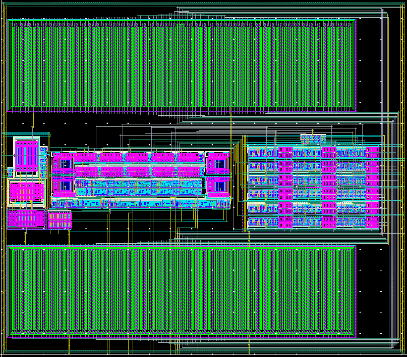
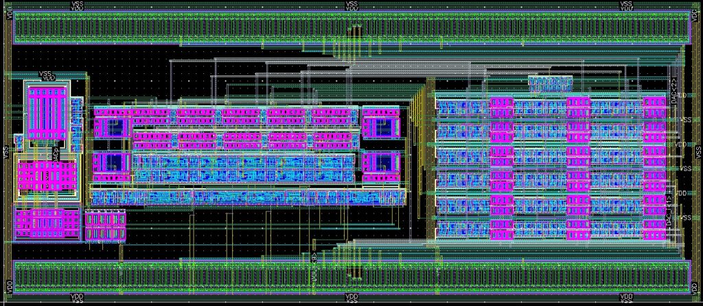
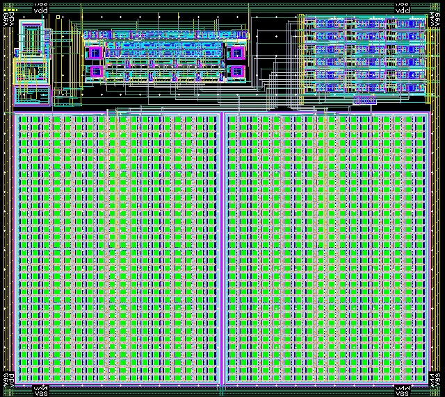
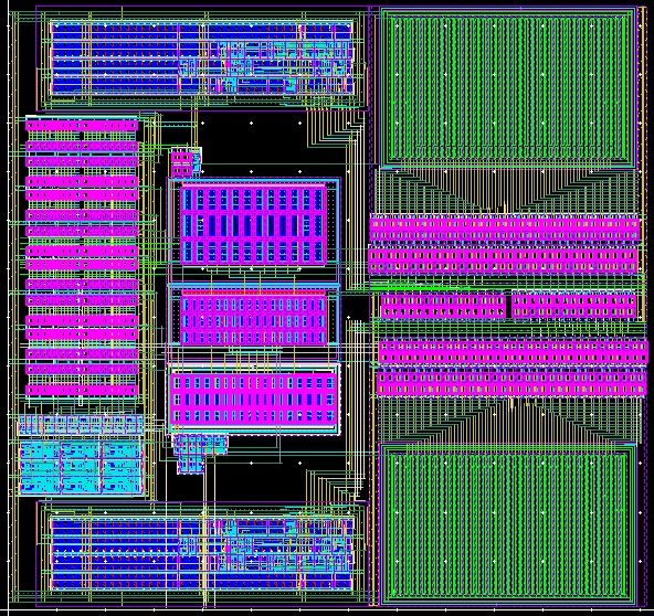
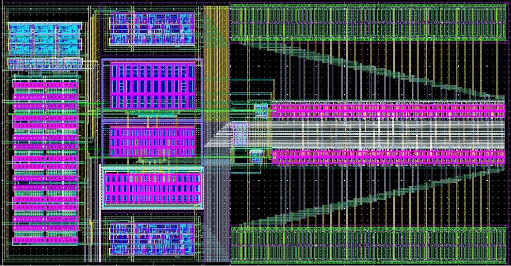
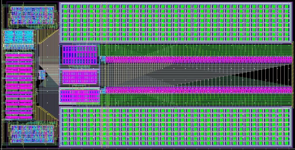
Differential Voltage-Mode A/D Converter (vADC) Asynchronous and Synchronous, including Sample-and-Hold
Typical Simulation Results Summary Table (Proof of Silicon 2Q25)
Refer to each cell data sheet below for more details (please see disclaimers).
| vADC Name | TSMC Fab Node | ~Size (µm× µm) | Bits | ~IDD (µA) | ENOB | Gain Error (%) | AINBW (KHz) | Conditions: aVDD~1v, VIN p-p ~1v, VREF p/n p-p~1v |
|---|---|---|---|---|---|---|---|---|
| vADC5_A_D | 65nm | 96x84 | 10 | 1 | 9.1 | 20% | 15 | Asynchronous, fS/H ≈ 40KHz |
| vADC5_A_F | 65nm | 94x41 | 10 | 1.2 | 9.2 | 30% | 15 | Asynchronous, fS/H ≈ 40KHz |
| vADC5_A_T | 65nm | 112x101 | 10 | 1.5 | 9.7 | 30% | 15 | Asynchronous, fS/H ≈ 40KHz |
| vAMP5_S_D | 65nm | 66x62 | 8 | 0.8 | 7.1 | 20% | 25 | Synchronous, fCLOCK ≈ 1MHz |
| vADC5_S_F | 65nm | 89x46 | 8 | 0.9 | 7.3 | 30% | 25 | Synchronous, fCLOCK ≈ 1MHz |
| vADC5_S_T | 65nm | 127x64 | 8 | 1.1 | 7.5 | 30% | 25 | Synchronous, fCLOCK ≈ 1MHz |
vADC5_A_D: Features (Silicon 2Q2025)
- View Datasheet
- 10-bit resolution, Low-Power, Differential voltage-input, Asynchronous vADC with S/H & Power-Down
- Optional: Digital output port (DOUT) can be serialized as needed.
- Digital power consumption reduces dynamically in steady-state VIN conditions, enabled by asynchronous vADC architecture.
- VINP and VINN terminals swing ~1v Peak-to-Peak around common mode voltage (e.g., VCM ≈ 5xVDD)
- Operating Condition Example: VREFP ≈ 1v and VREFN ≈ 0v
vADC5_A_F: Features (Silicon 2Q2025)
- View Datasheet
- 10-bit resolution, Low-Power, Differential voltage-input, Asynchronous vADC with S/H & Power-Down
- Optional: Digital output port (DOUT) can be serialized as needed.
- Digital power consumption reduces dynamically in steady-state VIN conditions, enabled by asynchronous vADC architecture.
- VINP and VINN terminals swing ~1v Peak-to-Peak around common mode voltage (e.g., VCM ≈ 5xVDD)
- Operating Condition Example: VREFP ≈ 1v and VREFN ≈ 0v
vADC5_A_T: Features (Silicon 2Q2025)
- View Datasheet
- 10-bit resolution, Low-Power, Differential voltage-input, Asynchronous vADC with S/H & Power-Down
- Optional: Digital output port (DOUT) can be serialized as needed.
- Digital power consumption reduces dynamically in steady-state VIN conditions, enabled by asynchronous vADC architecture.
- VINP and VINN terminals swing ~1v Peak-to-Peak around common mode voltage (e.g., VCM ≈ 5xVDD)
- Operating Condition Example: VREFP ≈ 1v and VREFN ≈ 0v
vADC5_S_D: Features (Silicon 2Q2025)
- View Datasheet
- 8-bit resolution, Low-Power, Differential voltage-input, Synchronous vADC with S/H & Power-Down
- Optional: Digital output port (DOUT) can be serialized as needed.
- Digital power consumption reduces dynamically in steady-state VIN conditions, enabled by asynchronous vADC architecture.
- VINP and VINN terminals swing ~1v Peak-to-Peak around common mode voltage (e.g., VCM ≈ 5xVDD)
- Operating Condition Example: VREFP ≈ 1v and VREFN ≈ 0v
vADC5_S_T: Features (Silicon 2Q2025)
- View Datasheet
- 8-bit resolution, Low-Power, Differential voltage-input, Synchronous vADC with S/H & Power-Down
- Optional: Digital output port (DOUT) can be serialized as needed.
- Digital power consumption reduces dynamically in steady-state VIN conditions, enabled by asynchronous vADC architecture.
- VINP and VINN terminals swing ~1v Peak-to-Peak around common mode voltage (e.g., VCM ≈ 5xVDD)
- Operating Condition Example: VREFP ≈ 1v and VREFN ≈ 0v
vADC5_S_F: Features (Silicon 2Q2025)
- View Datasheet
- 8-bit resolution, Low-Power, Differential voltage-input, Synchronous vADC with S/H & Power-Down
- Optional: Digital output port (DOUT) can be serialized as needed.
- Digital power consumption reduces dynamically in steady-state VIN conditions, enabled by asynchronous vADC architecture.
- VINP and VINN terminals swing ~1v Peak-to-Peak around common mode voltage (e.g., VCM ≈ 5xVDD)
- Operating Condition Example: VREFP ≈ 1v and VREFN ≈ 0v
